

Surface Treatment Vacuum Plasma Etching System
This is a device in the fields of semiconductor manufacturing, microelectromechanical systems (MEMS), optical coating and so on. It is a kind of dry etching equipment, which uses the ions generated in the vacuum environment to bombard the surface of the material, so as to achieve the purpose of accurately removing the material.
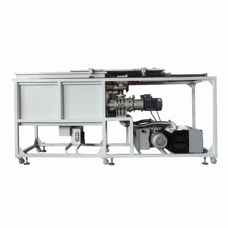
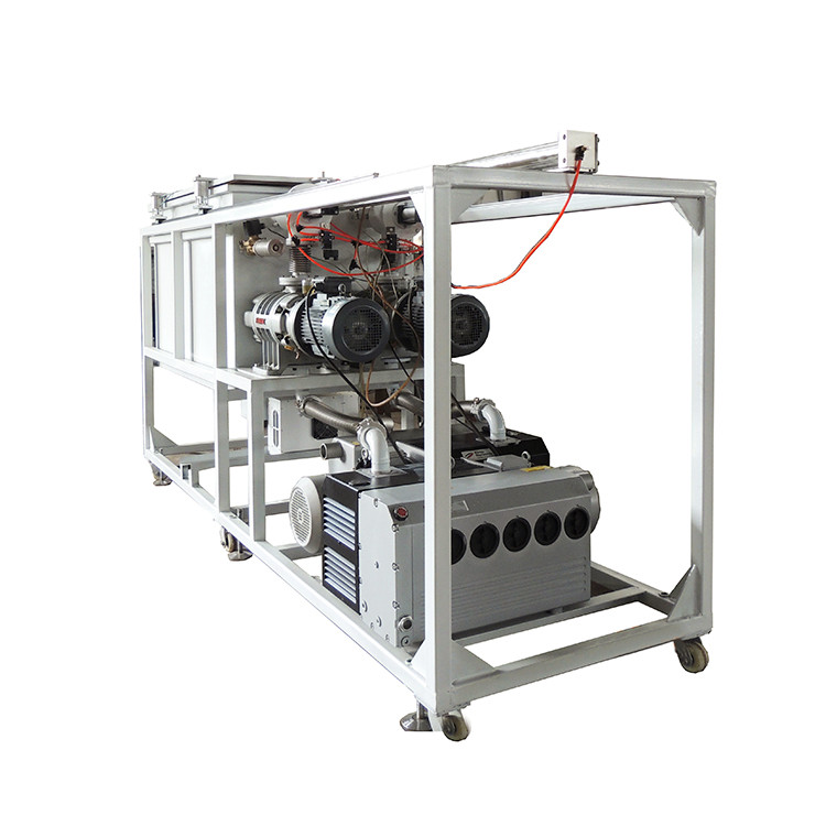
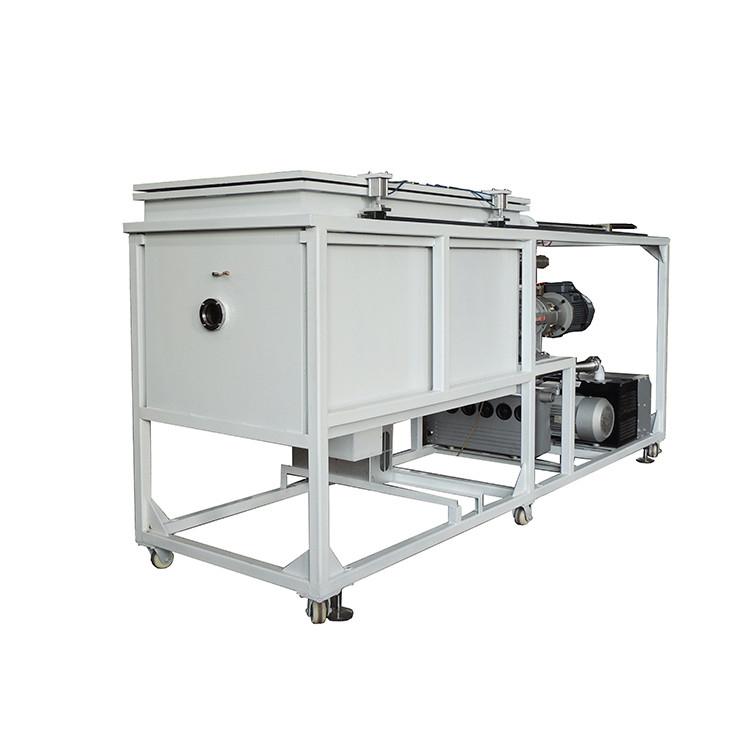
The plasma etching machine is mainly composed of the following systems:
Vacuum system
Vacuum chamber: usually made of stainless steel or aluminum, able to withstand high vacuum.
Vacuum pump system: including mechanical pump (rough pumping low vacuum) and molecular pump/cryopump (pumping high vacuum), which is used to establish and maintain the required high vacuum (usually up to 1010 to 1010 Pa) in the chamber.
Gas distribution system
Gas source: provide high-purity process gas (such as inert gas Ar2 for physical bombardment, or CF₄, Cl₂, BCl₃ for chemical assisted etching).
Mass Flow Controller (MFC): Accurately control the flow of various gases.
Gas lines and valves: precisely direct the gas into the chamber.
Plasma generation system
Radio Frequency (RF) Power Supply: The most commonly used energy source, typically at 13.56 MHz (industry standard free frequency).
Matchbox: It is used to adjust the impedance of the plasma, so that the energy of the RF power supply can be efficiently coupled into the plasma to reduce the reflected power.
Electrode: usually the lower electrode is connected to the RF power supply, the upper electrode is grounded, and the workpiece is placed on the lower electrode.
Control System
Computer and software: used to set and control all process parameters, such as vacuum degree, gas flow, RF power, etching time, temperature, etc., and monitor the whole process.
Optional:
Substrate temperature control system: heat or cool the sample stage to control the reaction rate.
End point detection system (EPD): By monitoring the plasma emission spectrum and other signals, it can judge whether the etching is completed in real time to ensure the consistency and accuracy of the process.
Coil (for ICP): In an inductively coupled plasma (ICP) source, a coil is used to generate a high-density plasma.
Applications
Semiconductor integrated circuit manufacturing: etching silicon, silicon dioxide, silicon nitride, metal and other thin films to form transistors, capacitors, interconnects and other microstructures.
Micro Electro Mechanical Systems (MEMS): processing of various micro sensors, micro actuators, micro structures (such as accelerometers, gyroscopes, microphones).
Photonics and optoelectronic devices: fabrication of distributed feedback lasers (DFB), optical waveguides, etc.
Nanotechnology: Preparation of nanowires, quantum dots and other nanostructures.
Materials science: used for sample preparation, such as thinning of TEM samples.
Advantages
Good anisotropy: it can etch the figure with steep side wall, and the precision is very high.
High resolution: it can reach the processing accuracy of nanometer level or even atomic level.
Clean and dry: no need to use wet chemical reagents, avoid washing and drying problems, less pollution.
High degree of automation: controllable process parameters, good repeatability, suitable for large-scale production.
Applicable to a variety of materials: metal, semiconductor, dielectric materials can be etched.